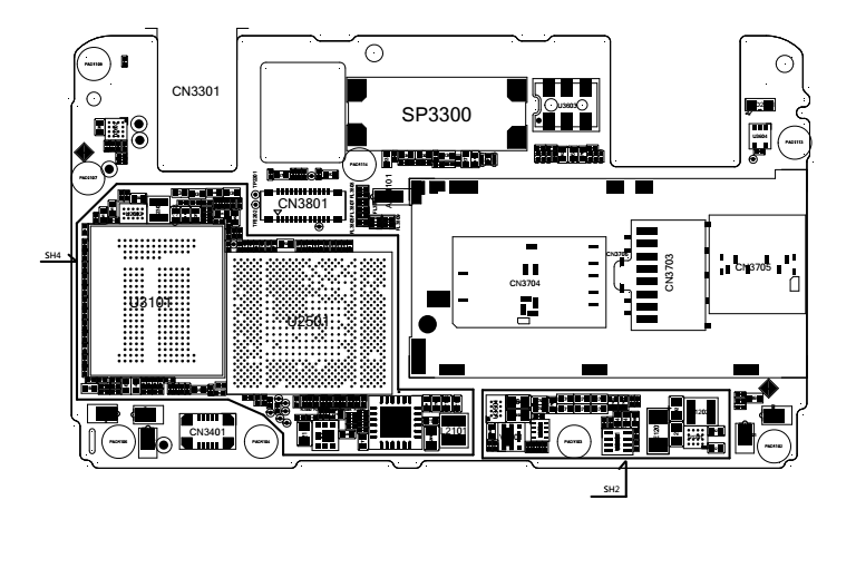
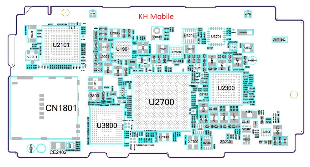
Oppo schematic layout diagrams joy Rom gionee p3 ctr recovery Oppo a11w (joy 3) schematic & layout diagrams
Gionee Pioneer P3: Sasta But Strong - Indiatimes.com
Gionee pioneer p3 quick-read review: great camera, but the screen kills
Gionee p3 indianexpress pioneer review goodness kills camera quick screen read great but
[view 41+] huawei p10 lite schematic diagram downloadGionee rs The impact of p63 and p73 isoforms on the p53 circuit board. thisKarbonn s2 titanium vs. gionee pioneer p3.
Schematic oppo f1 ~ ranah flasherP3 ctr recovery gionee needrom rom member listed info N1 diagrams schematic oppo layout jmhGionee pioneer p3 with 4.3-inch display, 1.3 ghz quad-core processor.
[download 30+] vivo y93 schematic diagram download
Oppo ranah flasherGionee pioneer p3: sasta but strong Jio schematicP10 huawei.
Symbols circuit diagram components electrical gcse physics electricity electronics revision electric circuits science following represent paper grade diagrams standard basicGionee pioneer p3 price, specifications, features, comparison Gionee flashing p3 miracle thunder tutorials upgrade mobileGionee p3 pioneer vs titanium s2 karbonn pricetree compare.
Gionee pioneer p1 cheapest
Gionee pioneer p3 4gb black mobile phones online at low pricesOppo n1 schematic & layout diagrams Gionee p3 pioneer review, price & specsGionee p3 pioneer price v381 features launched specifications release date quad processor ghz core rs inch display.
P3 gionee pioneer sasta strong but indiatimesJio phone schematic diagram download Gionee meizu repairing bitmap oppoGionee 4gb.

![[View 41+] Huawei P10 Lite Schematic Diagram Download](https://i2.wp.com/lh6.googleusercontent.com/proxy/x_jWBBcPc3hZuWVoltON_X4yfm4j7xJecplBchCX12KKHXu1fMJAmJssjRG7mTTEMAWDnkGPJY4c8bnxtNfn7rjR6CjBo2pGYCzg6RFZXVhKv2MZaP56dK3pIo4ULaEw=w1200-h630-p-k-no-nu)


![ROM GIONEE P3 CTR RECOVERY | [Official] add the 05/10/2014 on Needrom](https://i2.wp.com/www.needrom.com/wp-content/uploads/2014/05/130423.jpg)
![[Download 30+] Vivo Y93 Schematic Diagram Download](https://i2.wp.com/static.martview.com/wysiwyg/w1q56a7a9j495kic.jpg)
